Techniniai Dokumentai
Specifikacijos
Markė
Renesas ElectronicsProduct Type
Clock Buffer
Maximum Input Frequency
200MHz
Maximum Propagation Delay Time
350ps
Mount Type
Surface
Pakuotės tipas
SOIC
Kaiščių skaičius
8
Minimum Supply Voltage
3V
Maximum Supply Voltage
4.6V
Minimali darbinė temperatūra
-40°C
Maksimali darbinė temperatūra
85°C
Standards/Approvals
No
Serija
IDT23S05E
Automotive Standard
No
Kilmės šalis
Philippines
Produkto Aprašymas
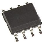
The Renesas Electronics zero delay clock buffer is a high-speed phase-lock loop (PLL) clock buffer, designed to address high-speed clock distribution applications. The zero delay is achieved by aligning the phase between the incoming clock and the output clock, operable within the range of 10 to 200MHz. The PLL feedback is on-chip and is obtained from the CLKOUT pad. In the absence of an input clock, it enters power down.

Ideate. Create. Collaborate
JOIN FOR FREE
No hidden fees!


Sandėlio informacija laikinai nepasiekiama.
€ 7,70
€ 0,77 Už kiekviena vnt. (tiekiama tuboje) (be PVM)
€ 9,32
€ 0,932 Už kiekviena vnt. (tiekiama tuboje) (su PVM)
Gamybinė pakuotė (Vamzdelis)
10

€ 7,70
€ 0,77 Už kiekviena vnt. (tiekiama tuboje) (be PVM)
€ 9,32
€ 0,932 Už kiekviena vnt. (tiekiama tuboje) (su PVM)
Sandėlio informacija laikinai nepasiekiama.
Gamybinė pakuotė (Vamzdelis)
10
| kiekis | Vieneto kaina | Per Vamzdelis |
|---|---|---|
| 10 - 20 | € 0,77 | € 3,85 |
| 25 - 45 | € 0,73 | € 3,65 |
| 50 - 90 | € 0,714 | € 3,57 |
| 95+ | € 0,702 | € 3,51 |
Ideate. Create. Collaborate
JOIN FOR FREE
No hidden fees!
Techniniai Dokumentai
Specifikacijos
Markė
Renesas ElectronicsProduct Type
Clock Buffer
Maximum Input Frequency
200MHz
Maximum Propagation Delay Time
350ps
Mount Type
Surface
Pakuotės tipas
SOIC
Kaiščių skaičius
8
Minimum Supply Voltage
3V
Maximum Supply Voltage
4.6V
Minimali darbinė temperatūra
-40°C
Maksimali darbinė temperatūra
85°C
Standards/Approvals
No
Serija
IDT23S05E
Automotive Standard
No
Kilmės šalis
Philippines
Produkto Aprašymas
The Renesas Electronics zero delay clock buffer is a high-speed phase-lock loop (PLL) clock buffer, designed to address high-speed clock distribution applications. The zero delay is achieved by aligning the phase between the incoming clock and the output clock, operable within the range of 10 to 200MHz. The PLL feedback is on-chip and is obtained from the CLKOUT pad. In the absence of an input clock, it enters power down.
Ideate. Create. Collaborate
JOIN FOR FREE
No hidden fees!